Analog Devices Inc. ADPA1116 GaN Power Amplifiers
Analog Devices ADPA1116 GaN Power Amplifiers feature a 39.5dBm saturated output power (POUT) power added efficiency (PAE) of 40% and a power gain of 23.5dB typical from 0.5GHz to 5GHz at an input power (PIN) of 16.0dBm. The RF input and output are internally matched and AC-coupled. A drain bias voltage of 28V is applied to the VDD1 and VDD2 pins, which have integrated bias inductors. The drain current is set using a negative voltage to the VGG1 pin. The ADPA1116 is manufactured using a gallium nitride (GaN) process and is available in a 32-lead chip scale package. The ADI ADPA1116 amps are specified for operation from -40°C to +85°C.Features
- Internally matched, 0.3GHz to 6GHz, 39.5dBm, GaN power amplifier
- RF input and RF output AC-coupled
- Integrated drain bias inductors
- 28V supply voltage
- 300mA quiescent current
- 39.5dBm typical from 0.5GHz to 5GHz (PIN = 16.0dBm) output power
- 23.5dB typical from 0.5GHz to 5GHz (PIN = 16.0dBm) power gain
- 40% typical from 0.5GHz to 5GHz (PIN = 16.0dBm) PAE
- 33.5dB typical from 0.5GHz to 5GHz small signal gain
Applications
- Electronic warfare
- Communications
- Radar
Functional Block Diagram

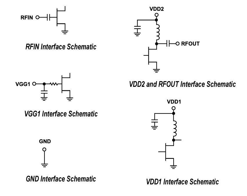
INTERFACE SCHEMATICS

Published: 2025-01-21
| Updated: 2025-02-24


