Texas Instruments LMK05028 Dual-Channel Network Synchronizer Clocks
Texas Instruments LMK05028 Low-Jitter Dual-Channel Network Synchronizer Clocks provide excellent hitless switching performance and advanced clock monitoring, meeting stringent timing requirements for communications infrastructure and industrial applications. A reduction in bit error rates (BER) offered in high-speed serial links results from the device's low jitter and high PSNR features. The device has two PLL channels that can select from any four reference inputs to synchronize its outputs and generates up to eight output clocks with 150fs RMS jitter.Flexible frequency configuration is achieved due to the programmable loop bandwidth for jitter and wander attenuation and fractional frequency translation options. Additional features include digital holdover, DCO mode with < 1 ppt/step for precise clock steering (IEEE 1588 PTP slave), and zero-delay mode for deterministic input-to-output phase offset. The Texas Instruments LMK05028 is fully programmable through I2C or SPI interface. It supports custom frequency configuration on power-up with the internal EEPROM or ROM, which is factory pre-programmable and in-system programmable.
Features
- Two independent PLL channels featuring
- 150fs RMS for outputs ≥100MHz jitter
- –112dBc/Hz at 100Hz offset for 122.88MHz phase noise
- 50ps phase transient with phase cancellation hitless switching
- Programmable loop bandwidth with Fastlock
- Standards-compliant synchronization and holdover using a low-cost TCXO/OCXO
- Any input to any output frequency translation
- Four reference clock inputs
- Priority-based input selection
- Digital holdover on the loss of reference
- Eight clock outputs with programmable drivers
- Up to six different output frequencies
- AC-LVDS, AC-CML, AC-LVPECL, HCSL, and 1.8V or 2.5V LVCMOS output formats
- EEPROM/ROM for custom clocks on power-up
- Flexible configuration options
- 1Hz (1PPS) to 750MHz on input and output
- XO: 10 to 100MHz, TCXO: 10 to 54MHz
- DCO mode: < 1ppt/step for fine frequency and phase steering (IEEE 1588 Slave)
- Zero delay for deterministic phase offset
- Robust clock monitoring and status
- I2C or SPI interface
- Excellent Power Supply Noise Rejection (PSNR)
- 3.3V supply with 1.8V, 2.5V, or 3.3V outputs
- –40°C to +85°C industrial temperature range
Applications
- SyncE (G.8262), SONET/SDH (Stratum 3/3E, G.813, GR-1244, GR-253), IEEE 1588 PTP slave clock, or optical transport network (G.709)
- Telecom and enterprise line cards
- Wireless Base Station (BTS), wireless backhaul
- Test and measurement, broadcast infrastructure, and medical ultrasound
- Jitter and wander attenuation, precise frequency translation, and low-jitter clock generation for FPGA, DSP, ASIC, and CPU devices
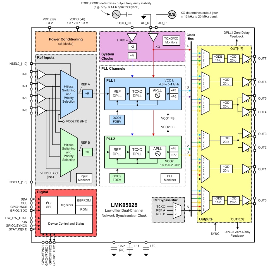
Functional Block Diagram

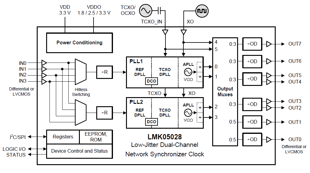
Simplified Block Diagram

Published: 2018-05-22
| Updated: 2023-01-18


